
Enphase publishes white paper on a gallium nitride chip that replaces two semiconductor switches with one in its solar microinverters
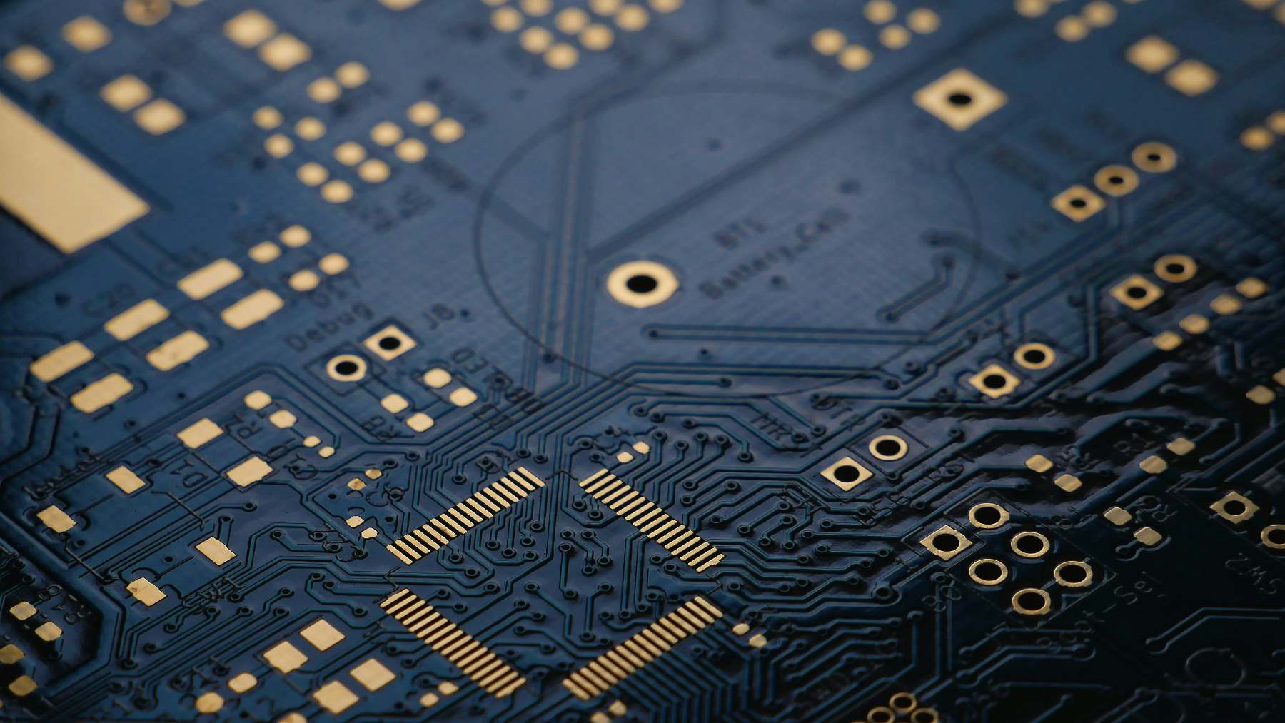
Inside every solar microinverter, a handful of semiconductor switches do the quiet work of turning sunlight into usable electricity. Enphase Energy has now published a technical white paper revealing that its IQ9 Series Microinverters replace the conventional pair of back-to-back transistors used for bidirectional switching with a single monolithically integrated gallium nitride device.
The shift is small in physical scale but significant in engineering logic. Power electronics sit at the invisible core of solar panels, home batteries, and EV chargers — and the materials inside them are starting to change.
Why the semiconductor inside your solar inverter matters
Power electronics — inverters, battery systems, EV chargers — depend entirely on semiconductor switches to convert and manage electricity. These devices toggle on and off millions of times per second, and their physical properties determine how much energy is lost as heat, how compact the hardware can be, and how well it handles demanding grid conditions.
According to the white paper, this consolidation reduces die area, gate charge, and component count compared with conventional back-to-back implementations.
Silicon has dominated this space for decades. Wide bandgap materials like silicon carbide (SiC) and gallium nitride (GaN) are emerging as superior alternatives for specific applications — SiC already common in high-power EV drivetrains and industrial systems, GaN having found its footing in compact consumer chargers for smartphones and laptops.
Enphase’s focus on a specialized variant — the monolithically integrated GaN bidirectional switch — marks a step beyond where mainstream GaN adoption currently stands.
One device where two used to be: how GaN BDS works
Conventional bidirectional switches are built from two back-to-back unidirectional transistors. Two separate devices, each handling one direction of current flow, working together to do a single job. It functions, but it carries inherent overhead in die area, gate charge, and component count.
A monolithically integrated GaN BDS achieves bidirectional voltage blocking within a single device structure — both directions handled by one piece of engineered semiconductor rather than a paired assembly. According to the white paper, this consolidation reduces die area, gate charge, and component count compared with conventional back-to-back implementations. Those device-level gains translate directly into measurable system-level performance improvements.
Four technical advantages Enphase highlights
The white paper organizes the case for GaN BDS around four specific benefits.
Higher efficiency. GaN BDS devices reduce switching and gate-drive losses during power conversion. In a microinverter running continuously across thousands of operating hours, even modest efficiency gains accumulate into meaningful energy output over the system’s lifetime.
Higher switching frequency. Lower gate charge allows the inverter to switch at higher frequencies, which permits smaller magnetics and passive filter components — physically shrinking the hardware without sacrificing performance.
Expanded voltage capability. The technology supports higher AC operating voltages, including 480 VAC three-phase commercial grid applications. This broadens the range of installations where Enphase hardware can operate without requiring separate product variants for different voltage environments.
Cost advantage. The monolithic structure reduces semiconductor die area relative to back-to-back designs. Smaller die area means lower manufacturing cost per device — a practical consideration when deploying at the scale Enphase operates.
Taken together, these advantages describe a technology that improves across multiple dimensions at once rather than trading one metric against another.
From rooftop solar to AI data centers: the broader roadmap
GaN BDS technology made its commercial debut in the IQ9 Series Microinverters, covering residential and commercial solar applications. That deployment established a production baseline for the device and validated its performance in real grid-connected hardware.
Enphase’s roadmap extends further. The white paper describes plans to incorporate GaN BDS into next-generation battery systems and the IQ Bidirectional EV Charger — two product categories where bidirectional power flow is central to the design challenge.
The most ambitious application described is the IQ Solid-State Transformer, intended for AI data center power infrastructure. That power module is expected to use higher-voltage GaN BDS and GaN unidirectional switch devices to support 800 VDC and ±400 VDC power systems — voltage levels well above anything in residential solar. The underlying physics that make GaN BDS useful in a rooftop microinverter are the same physics that make it relevant in a data center power module, which is precisely what makes this a platform technology rather than a single-product improvement.
Building the supply chain: from prototype to commercial device
A semiconductor technology’s value is only realized if it can be manufactured reliably and at scale. The white paper addresses this directly, describing Enphase’s work with semiconductor partners to move GaN BDS from early prototypes to commercially available devices.
Substrate management circuits, industry-standard packaging, and surge robustness are among the practical engineering concerns covered — the kind of details that determine whether a device survives real-world deployment rather than just laboratory conditions. Long-term reliability testing and qualification are identified as key milestones on the path to broader adoption. The paper also clarifies where GaN and SiC each belong in the power conversion landscape, treating them as complementary technologies suited to different voltage and frequency regimes.
Publishing this white paper signals that Enphase considers GaN BDS mature enough to discuss openly — and strategically important enough to anchor its next generation of products across solar, storage, EV charging, and data center infrastructure. The devices inside tomorrow’s energy hardware are already being designed today.

Carlos is an engineer with strong expertise in technical and industrial topics. He previously worked at international companies such as Siemens and is multilingual.
